
Wikipedia:Reference desk/Archives/Science/2016 December 12
| Science desk | ||
|---|---|---|
| < December 11 | << Nov | December | Jan >> | December 13 > |
| Welcome to the Wikipedia Science Reference Desk Archives |
|---|
| The page you are currently viewing is an archive page. While you can leave answers for any questions shown below, please ask new questions on one of the current reference desk pages. |
December 12[edit]
what is this circuit and how does it work?[edit]
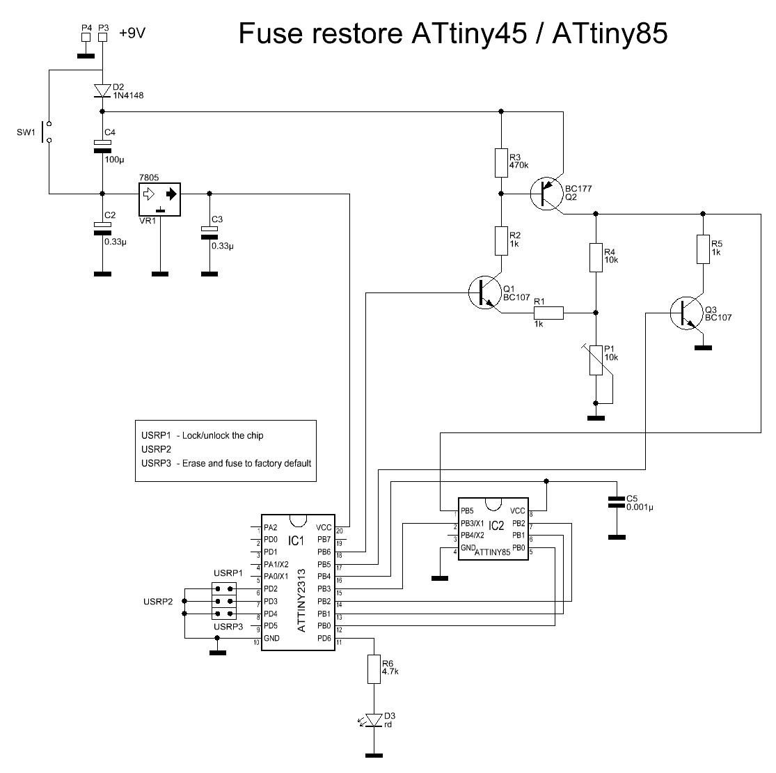
I mean the subcircuit around Q1 and Q2 here (ignore Q3.) It is supposed to regulate a higher voltage (around 18V) down to 12V when Q1's base is pulled high by the IO pin. The voltage (which is picked off of Q2's collector) is set by the 10k trimmer. I don't get the principle Asmrulz (talk) 15:47, 12 December 2016 (UTC)
- The circuit comprising Q1 and Q2 appears to form a voltage divider/regulator to drop the voltage of 18v on the large capacitor down to the required 12v for programming the chip. Looks very 'iffy' to me.--86.187.169.62 (talk) 19:18, 12 December 2016 (UTC)
- Of course the voltage is only applied when PB6 on IC1 is high.--86.187.169.62 (talk) 19:20, 12 December 2016 (UTC)
- I understood this much, I just would like to know how it does that. For example, I've a rough idea how this kind of stabilizer works (essentially a common-collector voltage buffer that buffers the resistor-Zener divider), but not the other circuit Asmrulz (talk) 22:52, 12 December 2016 (UTC)
- The voltage at PB 6 causes a base current in Q1. This results in a Q1 collector current that is fed to the base of Q2. Q2 has a high current gain( ~100) and this current is forced through the resistor chain to produce a voltage at the top of the chain. The chain is tapped at approximately half its resistance and this voltage fed back to the emitter of Q1. Q1 therefore acts as an error amplifier keeping the top of the resistor chain at approx twice (depending of the setting of the lower resistor) the voltage applied to its base. For more operational details, one would need to write down the equaitions. Does this help?--86.187.173.86 (talk) 13:43, 13 December 2016 (UTC)
- Should have said Q2 collector current is forced through the resistors.86.187.173.86 (talk) 13:45, 13 December 2016 (UTC)
- I can't say it clicked, but yes, that helps Asmrulz (talk) 14:24, 13 December 2016 (UTC)
- what determines how "stiff" the thing is?
This one is obviously not very stiff as it is pulled to ground by Q3 via a 1k resistordisregard this, the code never turns Q1 and Q3 on at the same time. The purpose of Q3 is to pull the second chip's PB5 to ground before the 12V are applied Asmrulz (talk) 14:24, 13 December 2016 (UTC)- To determine the stiffness of the voltage source, one would need to calculate its output resistance. I cant be bothered doing that, but, considering the large amount of open loop gain the circuit appears to have and the heavy negative feedback, I would think its pretty stiff. Of more concern may be the actual value of the output voltage which can be seen to be dependent on the voltage at PB6. Maybe thats why there's a trimpot in there that has to adjusted for jus the correct voltage.--86.187.168.14 (talk) 18:56, 13 December 2016 (UTC)
- I was reasonably intrigued by this circuit, so decided to a very quick and very dirty LT Spice analysis. The result of analysis showed that, for a PB6 voltage of 5v, the trimpot value should be about 6K to achieve 12v at the output. By loading the output until the nominal output voltage halved, I determined that the output resistance of the circuit was about 60 ohms. Hopefully, this should not peresent a problem in driving the chip programming pin.86.187.166.60 (talk) 01:12, 14 December 2016 (UTC)
- I understood this much, I just would like to know how it does that. For example, I've a rough idea how this kind of stabilizer works (essentially a common-collector voltage buffer that buffers the resistor-Zener divider), but not the other circuit Asmrulz (talk) 22:52, 12 December 2016 (UTC)